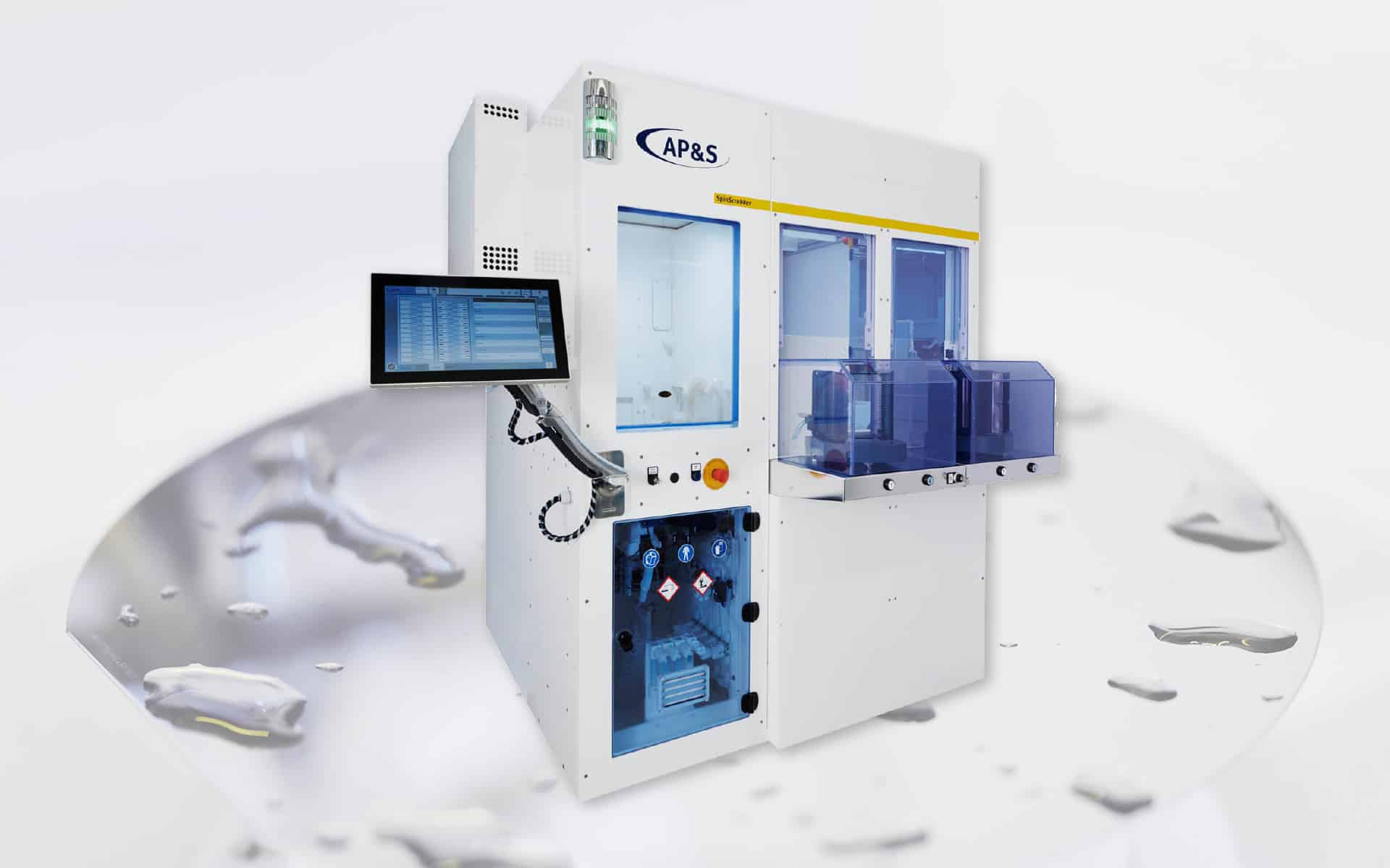
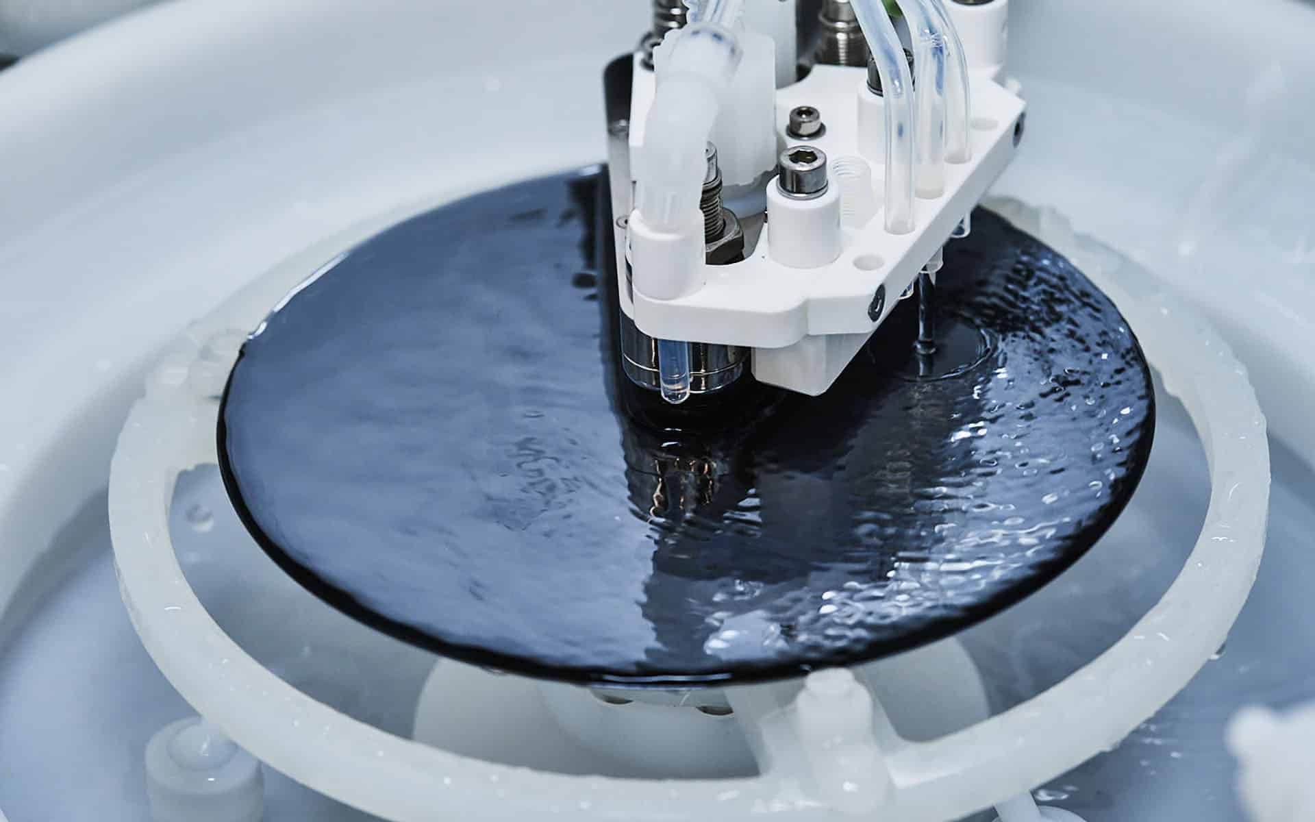
SpinScrubber
Wet-chemical single wafer process system for efficient particle removal on the surfaces of wafers, MEMS and photomasks
SpinScrubber
AP&S PRODUCTS
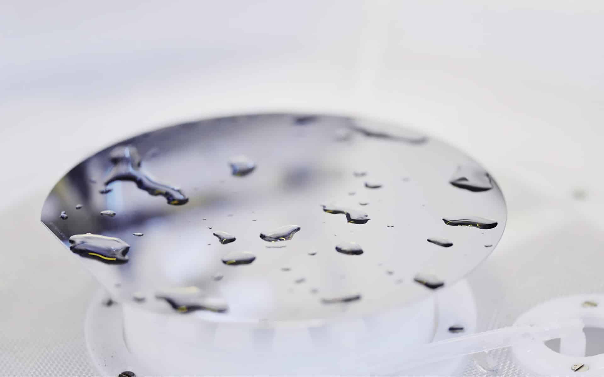
Efficient Particle Removal
The SpinScrubber single wafer system provides post grind, post polish, bevel clean and other chemical wet processes for substrate surfaces in semiconductor manufacturing.
Main Benefits
- Optimized CoC through low chemical and water consumption: chemical recovery and recycling included
- Parallel cleaning of the front and back side of the wafer is possible.
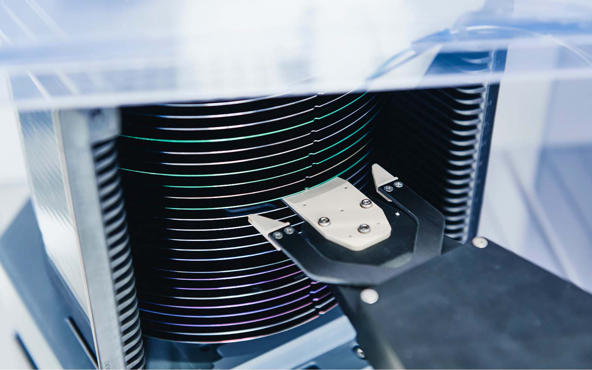
- Handling of thin wafers
- Up to two different cleaning media in one process tray - A tool demonstration in the AP&S DemoCenter is available.
Processes
- Post grind
- Post polish
- Post CMP
- Backside
- Reclaim
- Bevel clean
- TSV cleaning
Substrates
- Substrates
Wafers, MEMS, optoelectronics, photomasks, up to 9" and square substrates - Wafer material
Si, SiC, GaN, GaAs, sapphire, glass - Wafer sizes
up to 12″
Technical Features
- Easy configuration and flexible upgrading due to modular design
- Maximum safety for workers, plant and environment according to highest safety standards
- Optimized plant footprint, easy feed
- No expensive space for the Chemicals Management System in the clean room is required as it can be placed outside.
- Customized cleaning media on request
#CONTACT
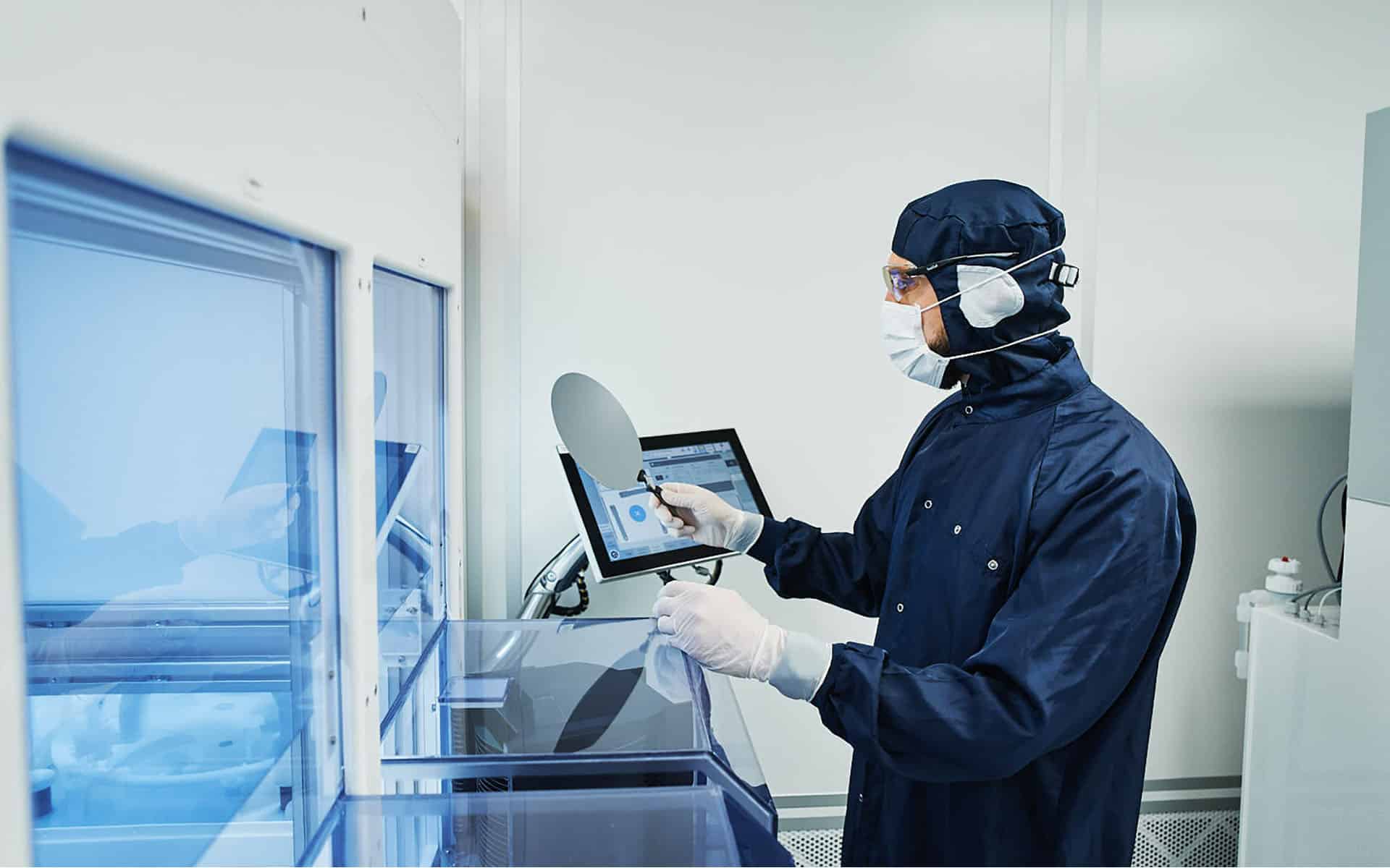
AP&S Products in Use
If you have any questions or would like to contact us, we look forward to meeting you.