CLEANING
Cleaning Processes
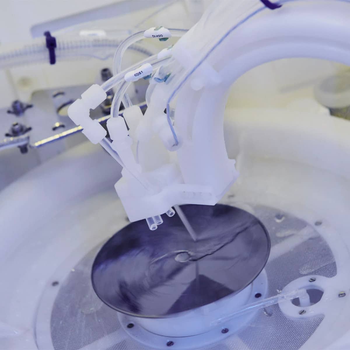
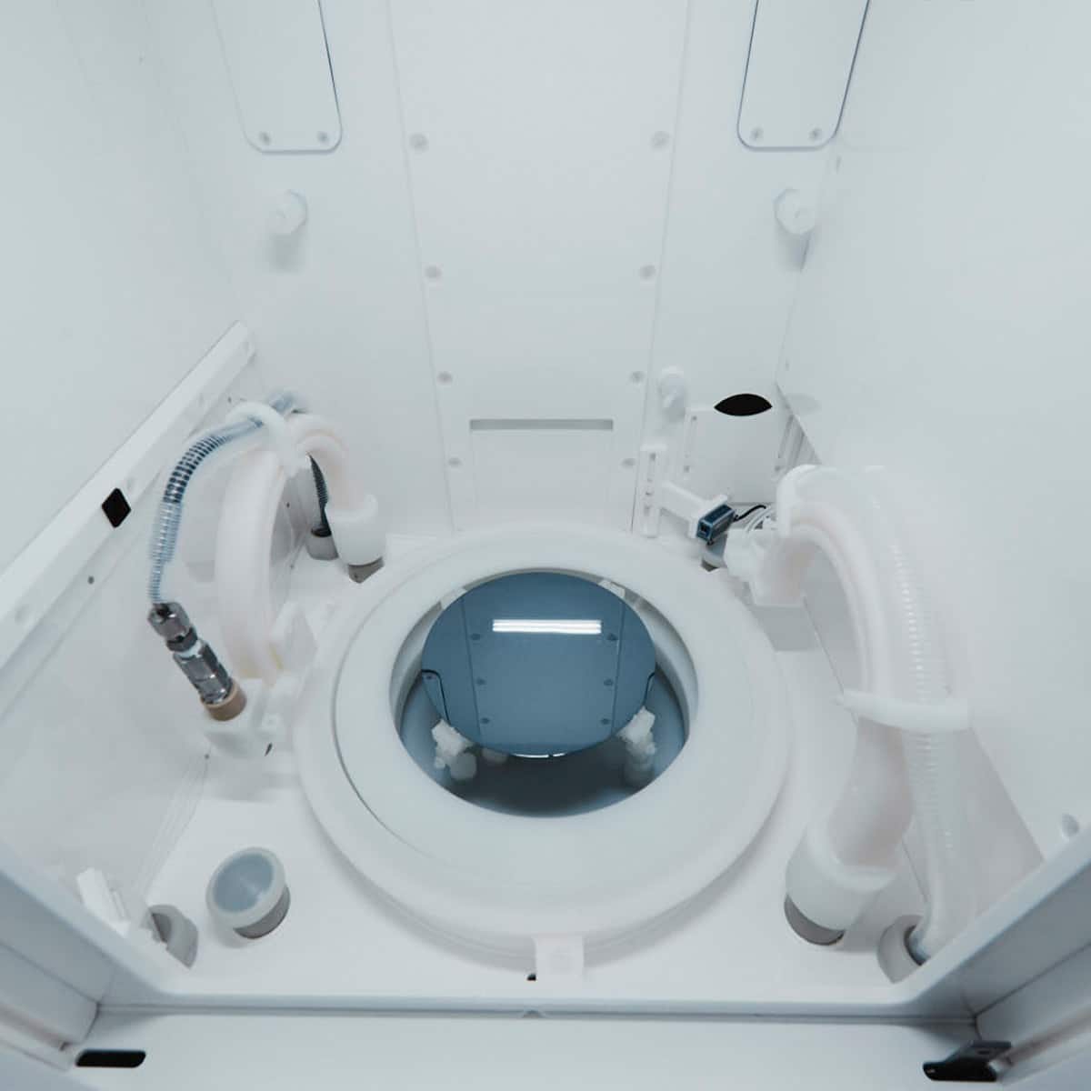
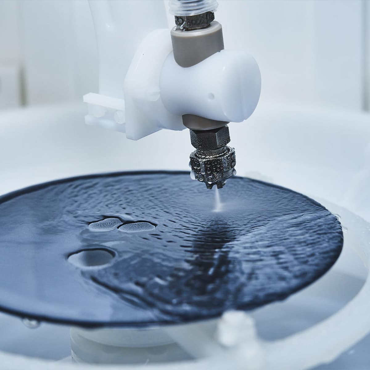
Cleaning processes using pure chemicals require adequate pure device solutions with advanced surface and structure interaction. The focus of the hardware design is on cleaning efficiency in variable structures with different aspect ratios. Effective removal of contaminants and particles down to the nanometer range is achieved.
Batch
Single Wafer
Production Supporting Equipment
Etching
Etching Processes
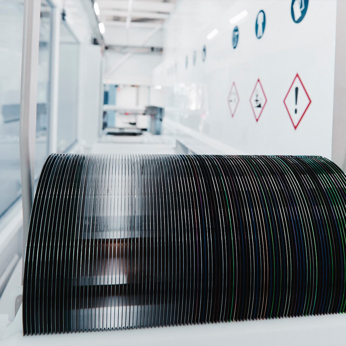
Etching processes of the various SC materials require hardware optimized for the high purity etching chemicals used. Low sigma variations of the etched structure dimensions across the chip, across the wafer and wafer to wafer are the main objective for wafer sizes up to 300 mm. Effective removal of etched materials in the structure is achieved by the optimized hydrodynamic flow conditions in the system, and AP&S drying concepts contribute to low particle content.
Batch
Single Wafer
RESIST STRIPPING
Resist Strip Processes
After etching, the structure is a permanent part of the top wafer layer. The resist that acted as an etch barrier is removed from the surface. Various chemicals (depending on the resist type) are used to remove the resists, while the hardware is optimized to create clean surface conditions and achieve low defect densities after stripping.
Batch
Single Wafer
Development
Resist Development
The resist structure is developed by the chemical dissolution of the non-polymerized resist area. The development forms a structure in the resist layer with the exact dimensions specified in the circuit development process. The hardware features are optimized for the chemicals used, since different chemicals are required for positive and/or negative resist layers.
Batch
Single Wafer
METAL ETCHING
Metal Etching Processes
Metal structure etching technologies for Al, Ti, W and others: complete removal of metals from device or monitor wafers for wafers up to 300 mm in diameter using hardware tailored to the specific chemicals required for each metal composite.
Batch
Single Wafer
Production Supporting Equipment
ELECTROLESS METAL DEPOSITION
Flip-Chip Bonding
Flip-chip bonding is of increasing importance for the further miniaturization of devices. Under-bump metallization (UBM) is performed with electroless deposition technology on Al alloy and Cu substrates. The UBM acts as an electrical connection, has a barrier function, and forms a mechanical connection between the substrate and the solder ball. Batch and single wafer processes are capable of meeting the equipment requirements and process stability necessary for mass production.
Batch
LIFT-OFF
Use of DMSO (Dimethyl Sulfoxide) & Megasonic
Metal lift-off is a patterning process that eliminates the etch variation component. The wafers are processed in one development step, leaving a hole in the resist layer where the deposited layer is above the resist and in the opening. By using ultrasound, the deposited layers are removed with the resist, leaving the desired structure on the wafer surface.
Single Wafer
DRYING
Wafer Drying
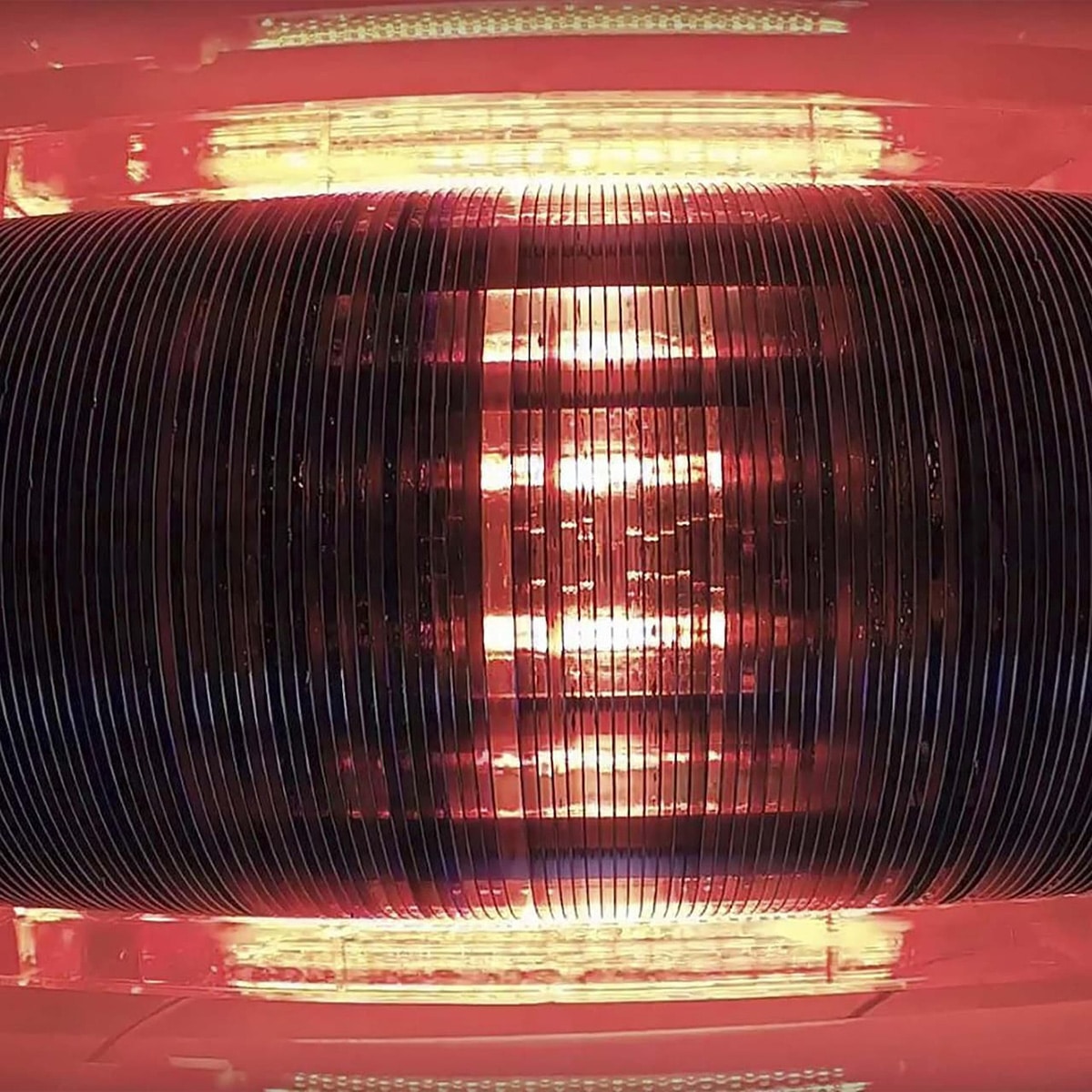
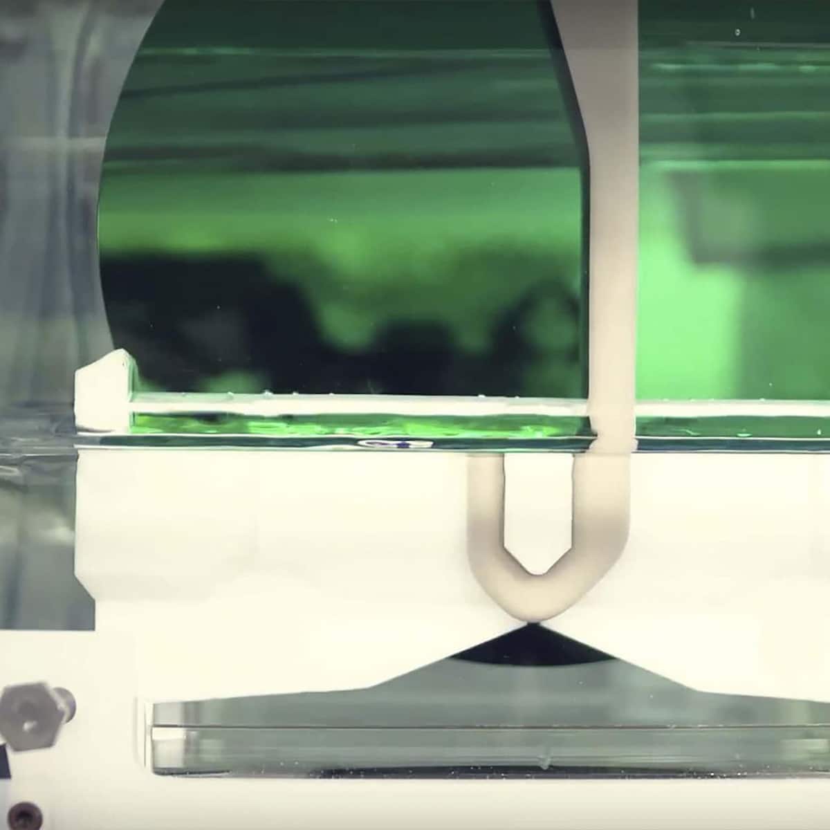
Water surface tension has a unique nature when wafers are slowly pulled through a water surface: The tension pulls the water away from the surface, leaving the wafers dry. By using additional IPA and N2, this effect is enhanced at the water-water interface by creating a strong surface tension gradient (Marangoni drying).

