ENTRY
Research & Development
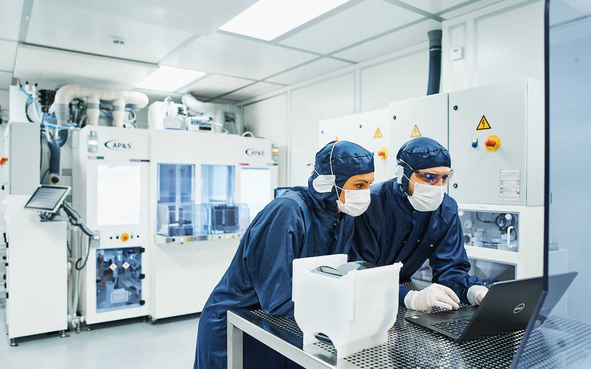
An investment in a wet process plant is an important decision in which many relevant aspects and complex interrelationships must be taken into account. AP&S supports you efficiently in the decision-making process in our DemoCenter.
Development
AP&S DemoCenter
Are you looking for a wet process plant that perfectly meets your specific requirements? Our team of experienced process engineers will help you to fully clarify all relevant decision criteria and to prepare the purchase decision in the best possible way.
The AP&S DemoCenter takes care of process development and modification for standard as well as innovative semiconductor materials such as silicon (Si), silicon carbide (SiC), gallium nitride (GaN) or indium phosphide (InP). Here in the wet process lab you will get a concrete comparison of process performance and parameters on different wet process equipment as well as an analysis and recommendation for drying processes for deep structures, MEMS and TSVs.
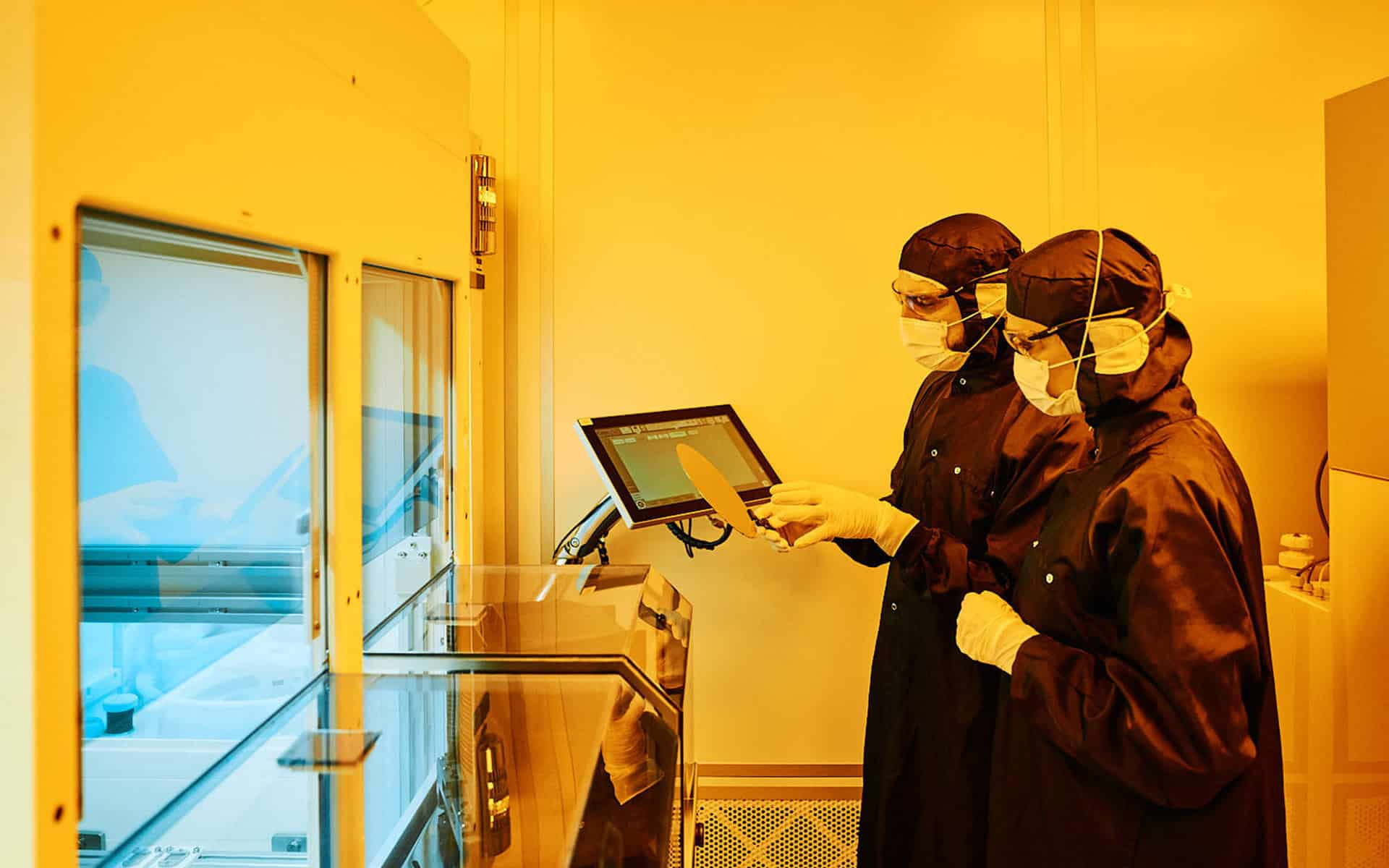
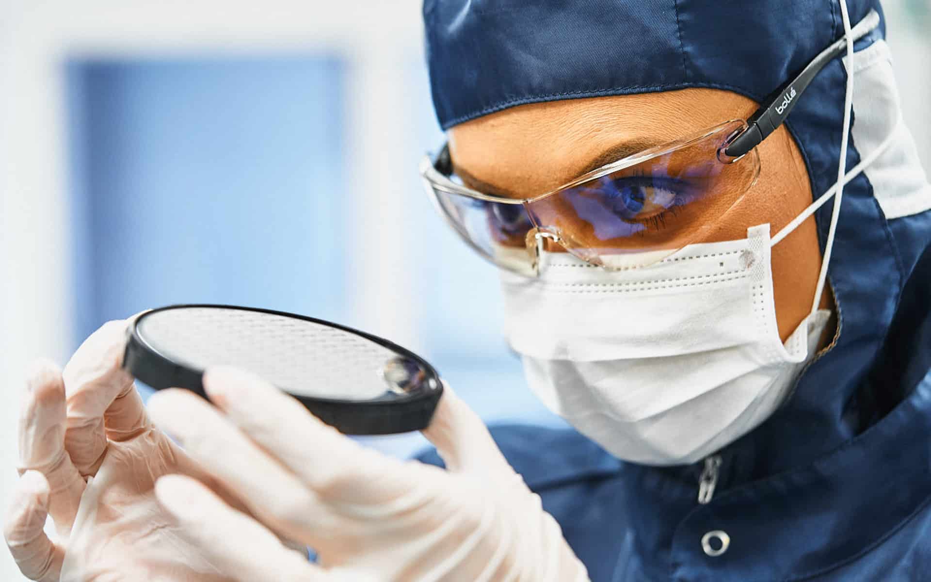
With 66 square meters of ISO 5 cleanroom environment and over 25 chemical wet processes in our line, you will receive comprehensive support for a sound investment in your next wet process equipment.
LIVE OPERATION
Process Experience - "Deep Dive"
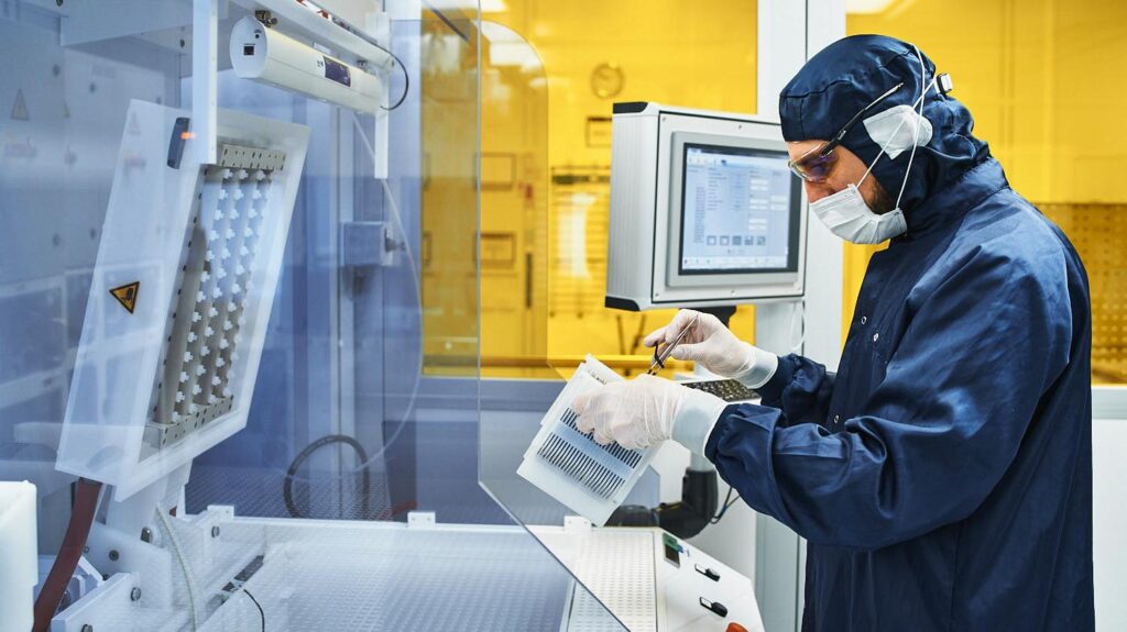
In the AP&S DemoCenter you can experience chemical wet processes in live operation. Our highly qualified process engineering team will explain all details of the wet process plants to you. You will receive a comprehensive test report with complete parameters of the process setup as well as recommendations for a plausible plant configuration that is precisely tailored to your needs and requirements.
Optimization
Quality Check
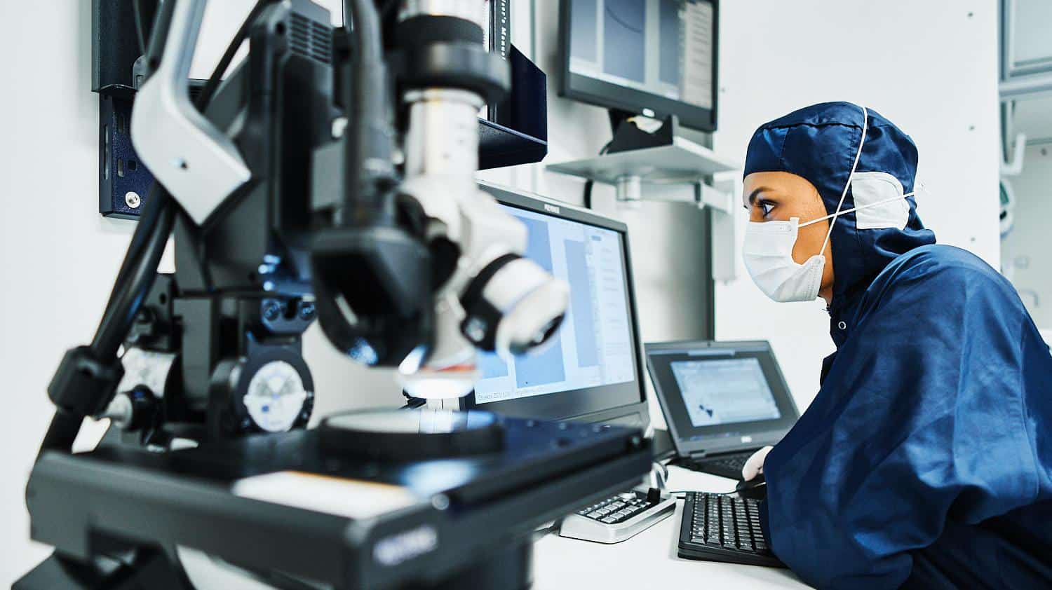
The AP&S DemoCenter is equipped with the latest testing and analysis equipment, such as the syringe liquid sampling system SLS1100 and particle measuring device LASAIR III 110. In addition, we run joint development projects with renowned research institutes worldwide.
Efficiency
Time & Cost Savings
Before the start of production, we offer you an in-house process evaluation including process parameter definition, calculation of throughput and chemical consumption.
ON SITE
Trust
When visiting the AP&S DemoCenter, you will not only get to know our wet process equipment and its performance, but also gain a comprehensive impression of our company headquarters. Here you will learn how we work and meet the people behind AP&S.
SINGLE WAFER DEMOS
Wet Process Demonstrations - Single Wafer
General
- Fully automated double chamber plant
- Processing of substrates up to a maximum of 300 mm or 9×9 inches
- Handling of 6 and 8 inches substrates by means of vacuum or edge grippers
- Wafer mapping
- 7 chemical systems, two systems for applications up to a maximum of 70° C
- Drain separation for both process chambers
- Various types of chucks: vacuum chucks, low contact chucks, clamp chucks, frontside protection chucks, etc.
- Programmable chuck height
Process Chamber 1
- Processes: metal lift-off, PR strip, solvent processes
- Megasonic / megasound nozzle
- High pressure cleaner for solvents and/or DI-H2O
- Various puddle / spray nozzles
- Rear side protection with DI-H2O or N2
Process Chamber 2
- Processes: metal etching, various etching processes (dHF max. 0.5%), mask cleaning, substrate cleaning
- Megasonic / megasound nozzle
- Wafer coating system
- Various puddle / spray nozzles
- Rear side protection with DI-H2O or N2
Possible supplements
- Immersion station
- Ultrasonic cleaning module
- Endpoint detection system
BATCH DEMOS
Wet Process Demonstrations - Batch
General
- NID dryers for drying standard substrates, Taiko, MEMS, thin wafers, etc.
- IPA (isopropyl alcohol) concentration monitoring
- Processing of substrates up to 300 mm or 9×9 inches with various substrate thicknesses
- Batch size maximum 25 substrates per box/carrier
- Different process carriers possible (high/low profile, LMC, customer-specific carriers)

