The company based in Donaueschingen (Aasen) announces its entry into the US market. In response to customer inquiries from the USA, AP&S has now taken this step and hired its first employees in April.
AP&S International GmbH builds wet process equipment for the manufacture of microchips and is therefore active in the semiconductor industry. The USA remains a key market for German mechanical engineering and semiconductors have also become the focus of geopolitical interests. In addition, the "Chips Act" is attracting chip companies and suppliers to the USA.
With a gross domestic product of around 27.97 trillion US dollars (2024), the USA is the largest economy in the world. The opportunities for companies in the land of opportunity are correspondingly great.
One of the drivers for investment in the USA is the expected boom in electric cars. The production of SiC chips can guarantee a greater range and more efficient charging processes. This technology is also being strongly promoted in the USA.
AP&S, which currently has 250 employees worldwide, has the know-how for market expansion thanks to over 20 years of expertise in the market. Most potential customers based in the USA already know the company from existing contracts with other locations around the world. This has already resulted in the first major order for five systems, which will be built for a customer in the USA by mid-2025.
The systems ordered for the USA are both production-supporting equipment and batch systems (several wafers* are processed at the same time), some standardized, some customized to customer requirements. In order to test and prepare customer processes realistically, the company has a DemoCenter in which laboratory tests are carried out so that the wet processes can then be prepared precisely for the system. Operators of the systems are trained in the in-house training center, the AP&S Academy, to prevent a shortage of skilled workers.
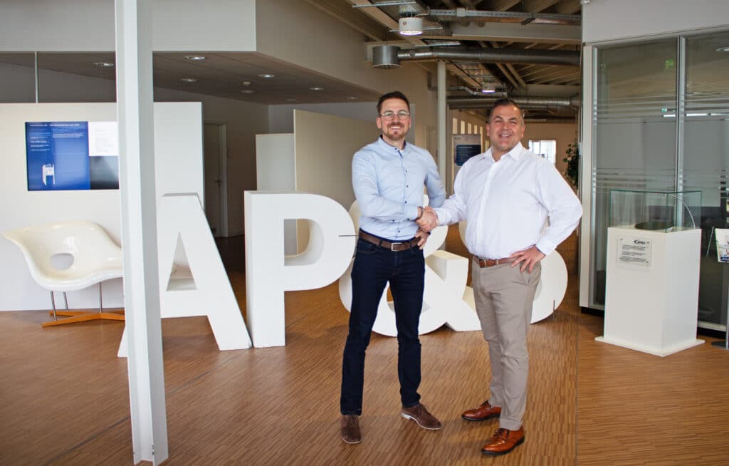
Tobias Bausch, CMO&CTO of AP&S International GmbH, is now also responsible for the new location as CEO, AP&S US Inc. He and his employees will continue to expand the company there. "Opening up the US market is a major challenge but also an opportunity that we are very much looking forward to. The needs of our existing and new customers in the USA are very important to us and we will demonstrate the "Made in Germany" brand here with commitment and drive," says Tobias Bausch.
For AP&S, this step is a milestone in its successful history following its foundation in 2003 by Horst Hall and Alexandra Laufer-Müller (CEO). "This step underlines our commitment to offer our customers worldwide first-class products and to always be close to the market," says Alexandra Laufer-Müller. *A wafer is a thin slice of semiconductor material (usually silicon).