SpinMetal
Metal etching system with endpoint detection for top-level process control
SpinMetal
AP&S PRODUCTS
Etching of Metal Layers
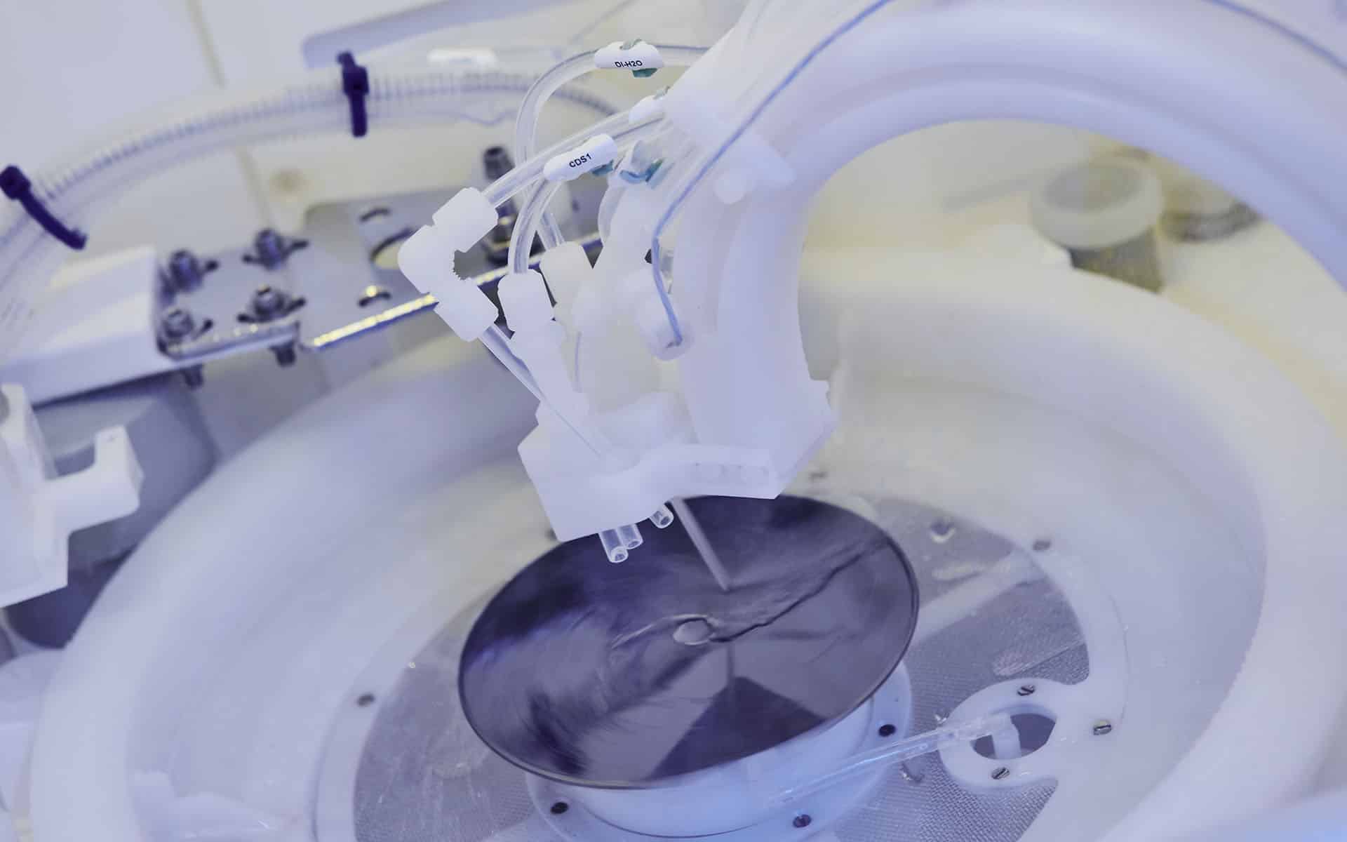
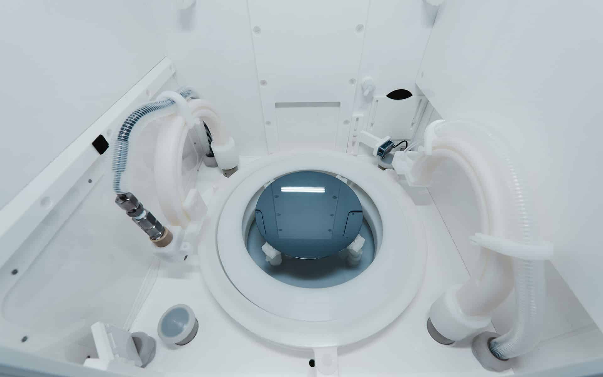
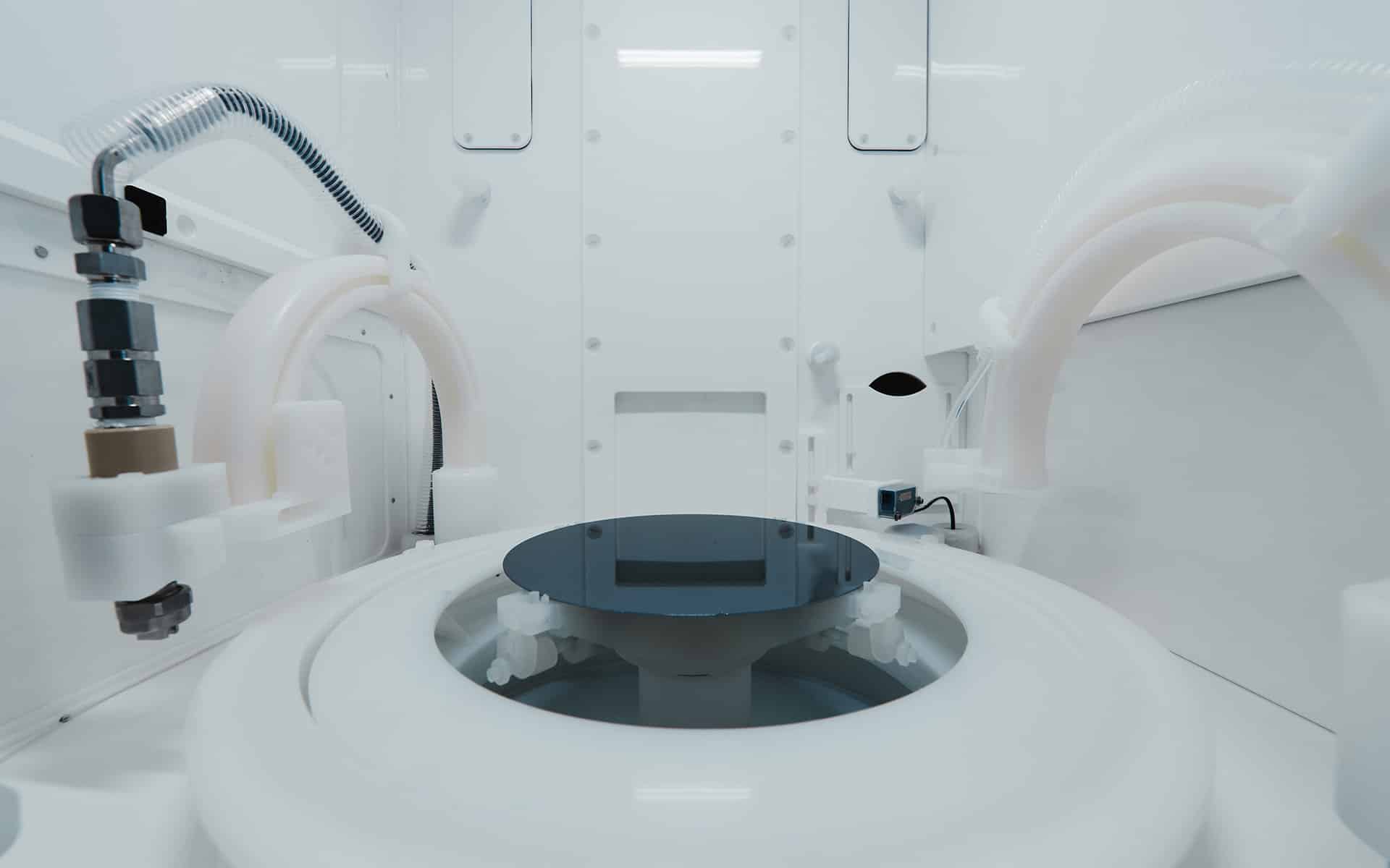
This single wafer system achieves optimum process results when etching metal layers of a wide variety of materials.
Main Benefits
- Endpoint detection for highest reliability and process control:
1. Less over-processing time required to fully etch the layer (i.e. over-etching)
2. Less impact on other layers
3. Stable uniformity from wafer to wafer
4. Significant reduction of chemical consumption possible
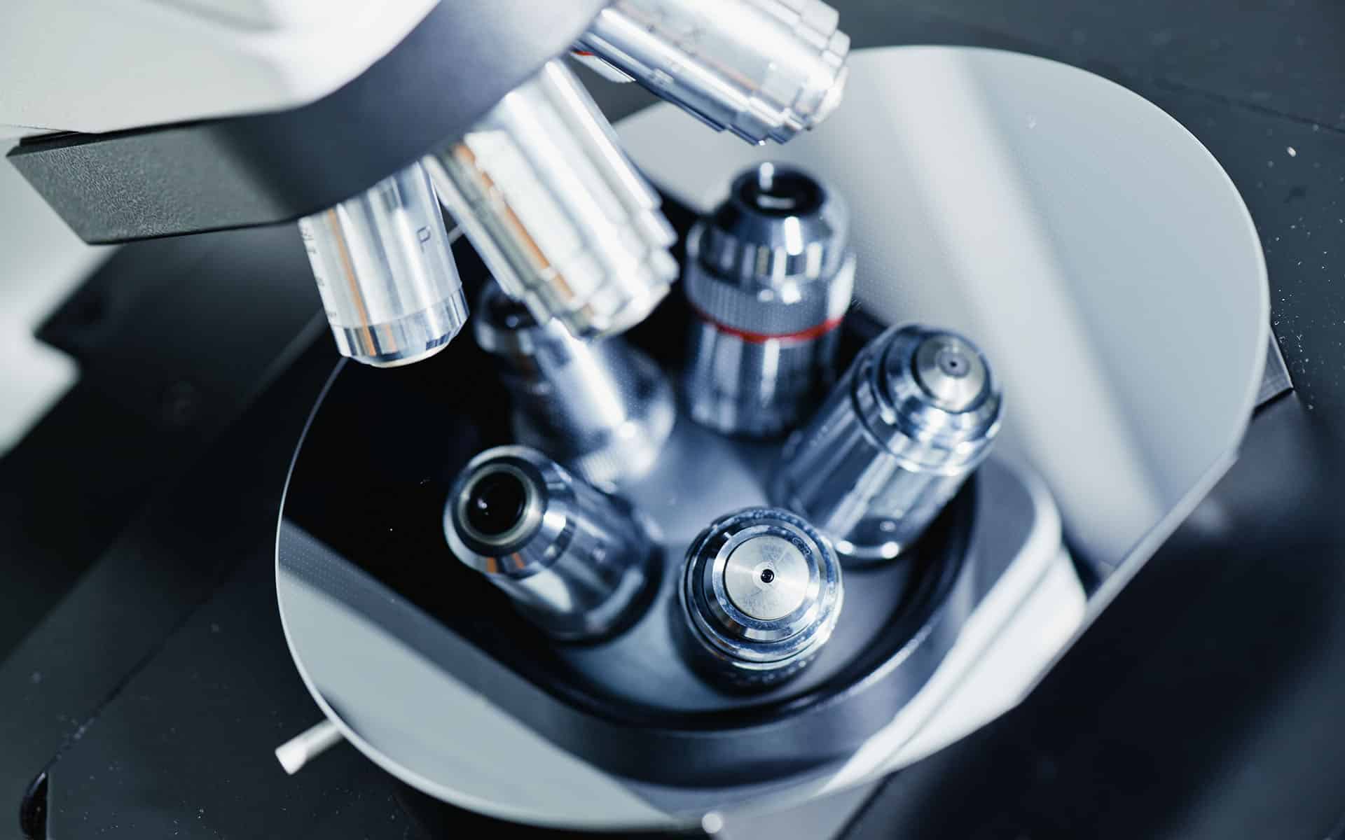
- Up to 6 different etching media
- Backside protection of the wafers
- A plant demonstration in the AP&S DemoCenter is available.
Processes
The SpinMetal system is suitable for etching metal layers of the following materials: nickel-chromium, nickel, copper, cobalt, aluminum, gold, titanium, titanium tungsten, silver, bismuth antimonide and others.
Substrates
- Substrates
Wafers, MEMS, optoelectronics, photomasks, up to 9" and square substrates - Wafer material
Si, SiC, GaN, GaAs, sapphire, glass - Wafer sizes
up to 12″
Technical Features
- Easy configuration and flexible upgrading due to modular design
- Maximum safety for workers, plant and environment according to highest safety standards
- Optimized plant footprint, easy feed
- No expensive space for the Chemicals Management System required in the clean room, as this can be positioned outside. Link to the Mini Chemical Systems
#CONTACT
AP&S Products in Use
If you have any questions or would like to contact us, we look forward to meeting you.